
Advanced spectroscopy
Atomic Resolution and Lorentz Analysis
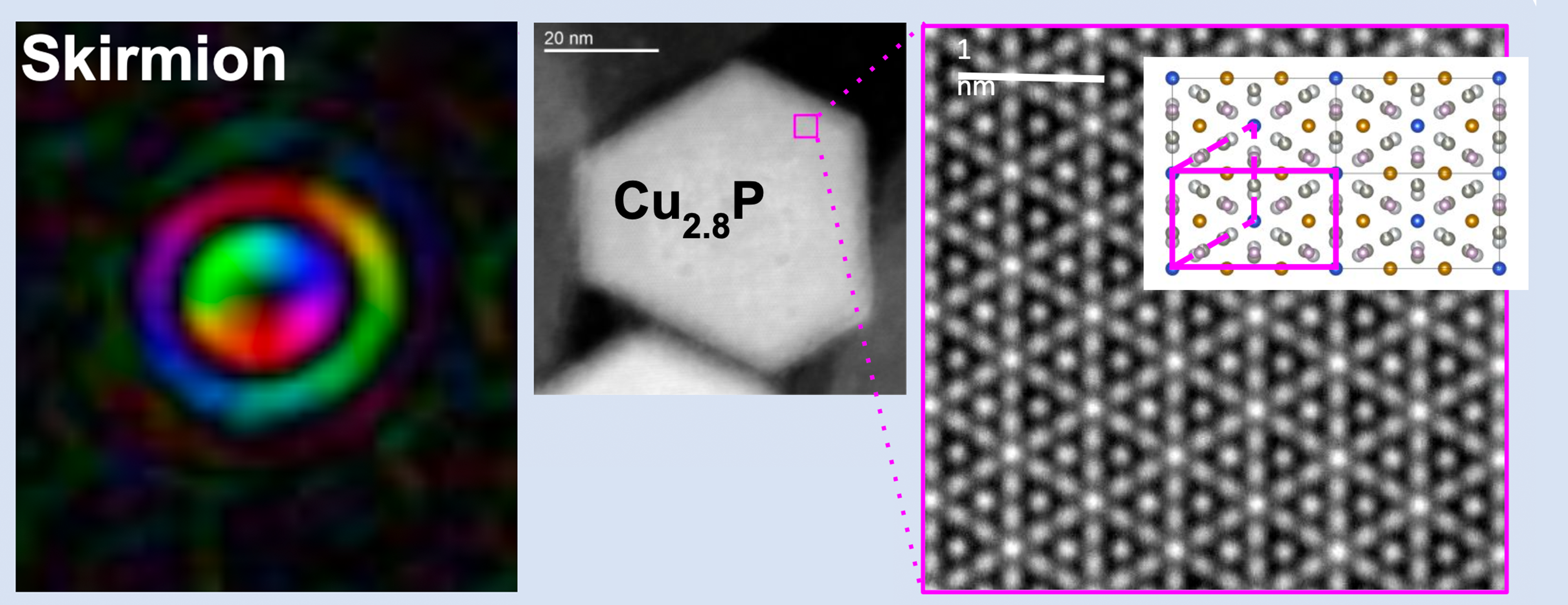
Advancements in atomic-resolution imaging and Lorentz microscopy have revolutionized our ability to study material structures and magnetic properties at the nanoscale. High-Resolution Scanning Transmission Electron Microscopy (HR-STEM) allows us to visualize atomic arrangements with exceptional clarity, offering invaluable insights into material properties and behaviors.
Dynamic scattering simulations play a crucial role in complementing HR-STEM by modeling electron interactions within materials. These simulations account for multiple scattering events, enhancing the accuracy of structural interpretations and enabling precise modeling of even the most complex materials.
Lorentz microscopy provides a powerful tool for reconstructing magnetic fields at the nanoscale. By analyzing phase shifts in electron waves as they pass through magnetic materials, this technique maps magnetic domain structures, deepening our understanding of magnetic phenomena and aiding in the development of advanced magnetic materials.
Structural analysis and modeling are key to interpreting data from these techniques. By combining experimental observations with theoretical models, researchers gain a comprehensive understanding of material properties, paving the way for the design of materials with tailored functionalities.
For example, Bertoni et al. (ACS Materials Letters, 2019) employed HR-STEM and electron energy-loss spectroscopy (EELS) to investigate the bandgap in orthorhombic cesium lead halide perovskite (CsPbBr₃) nanosheets. Their findings revealed a bandgap increase in nanosheets thinner than 10 nm, highlighting the effects of quantum confinement in these materials. Similarly, Brescia et al. (Nanoscale Horizons, 2020) studied twisted double-bilayer WSe₂, providing insights into the interaction effects and superconductivity signatures in two-dimensional materials. Their research contributes to the development of innovative electronic and optoelectronic devices.
These studies underscore the critical role of advanced imaging and analysis techniques in nanoscience, enabling the exploration of material properties at unprecedented resolutions and driving the development of next-generation technologies.
EELS SPECTROSCOPY
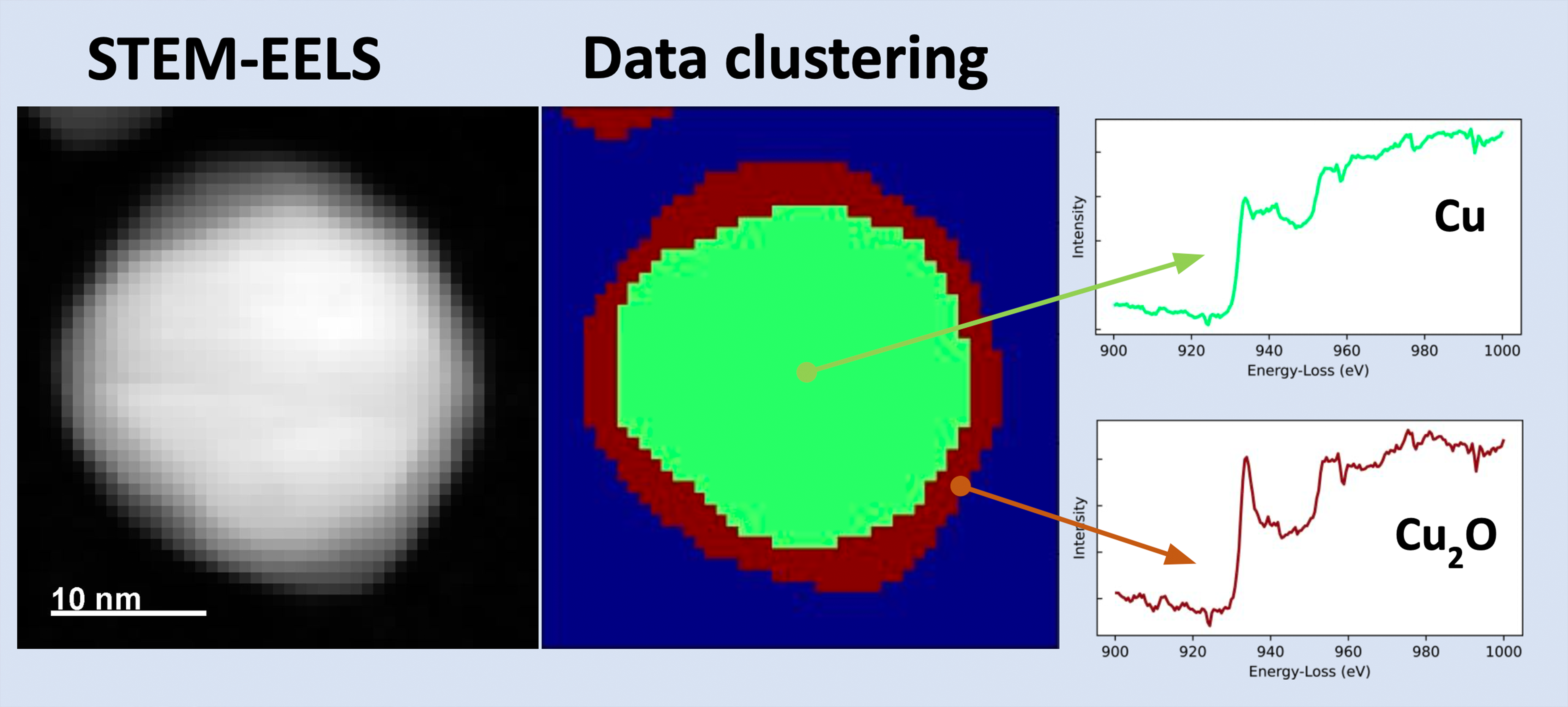
Electron Energy-Loss Spectroscopy (EELS) is a powerful technique for probing the chemical and physical properties of materials with high spatial resolution. One of its key applications is the decomposition of EELS spectra using Multivariate Statistical Analysis (MSA), which facilitates precise chemical mapping. This approach enables the identification and spatial localization of different chemical elements and compounds within a sample, offering valuable insights into its composition and structure.
Looking ahead, advancements in EELS are focused on developing automated tools for data acquisition and analysis. These tools aim to streamline the experimental workflow by providing real-time chemo-physical information about the sample as the experiment is conducted. By integrating advanced data processing algorithms and machine learning, these developments promise to enhance the efficiency and accuracy of EELS, making it a more robust tool for materials characterization and analysis.